Videos
Design a circuit which produces the transfer function
Design a circuit which produces a transfer function of
Explanation of Solution
Given data:
The given transfer function is,
Calculation:
The transfer function of the circuit is,
Equation (1) is written as,
For numerator:
From equation (2), for the numerator
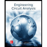
The Figure 14.39 (b) in the textbook, that shows a cascade two stages of the circuit with a zero at
From the Figure 1, a single zero can be written as,
Substitute
Consider the value of
Substitute
Transfer function:
The input impedance of the cascaded circuit in Figure 1 is,
Then, write the Formula for the transfer function for the cascaded two stage amplifier.
Substitute
Thus, consider that the transfer function for
Substitute 50 for
Completing the design by letting
Thus, the final design of the circuit is,
For denominator:
From the transfer function shown in equation (2), it has two repeated poles at
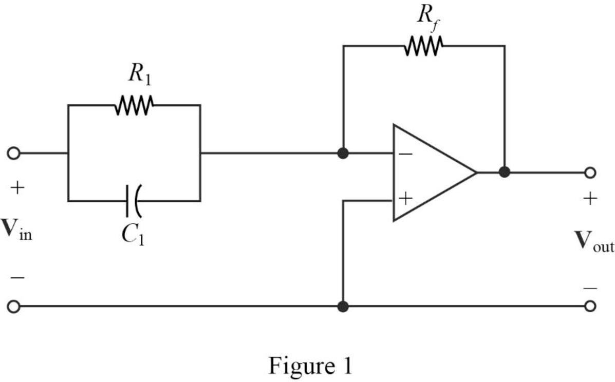
The Figure 14.39 (a) in the textbook, that shows a cascade two stages of the circuit with pole at
Consider that the cascaded circuit for the two poles representation as shown in Figure 2.
From Figure 2, and the denominator of given transfer function a first pole at
Where, the circuit parameters are considered as
Substitute
Let arbitrarily consider
Substitute 13.3 for
Transfer Function:
Find the feedback impedance of the cascaded circuit in Figure 2.
Write the formula for the transfer function of the cascaded circuit in Figure 2 as follows
Substitute
Therefore, consider the transfer function
Substitute 75 for
Completing the design by letting
Since, two repeated poles are at same
Therefore, the complete transfer function for the denominator part is,
Substitute
Thus, the final design of the two stages cascaded circuit for the denominator part is,
Thus, the overall transfer function of the complete circuit using the transfer function of numerator
Substitute
The input will be inverted, and adding an inverting amplifier with gain of 1 to provide the transfer function as follows.
Conclusion:
Thus, a circuit is designed which produces a transfer function of
Want to see more full solutions like this?
Chapter 14 Solutions
Engineering Circuit Analysis
Additional Engineering Textbook Solutions
Fundamentals of Electric Circuits
Electric Circuits. (11th Edition)
Principles Of Electric Circuits
Electronics Fundamentals: Circuits, Devices & Applications
ELECTRICITY FOR TRADES (LOOSELEAF)
Fundamentals of Applied Electromagnetics (7th Edition)


- 4. Write the state space representation for the following transfer function R(s) 100 54+ 20s3+ 10s2+ 7s+ 100arrow_forwardShow that the below reduced transfer function (Figure 1) can be written as 3 s +1 C(s) R(s) R(s) + 2 4 s² +25¹ +2s S 1 S Figure 1 S + C(s)arrow_forwardA second order system is described by the transfer function G(s) = 100/(s*s+ 17s+100). The pic time of %3D a unit step response is: Select one: a. None of the above O b. 0.59 c. 0.39 sec O d. 0.31 sec O e. 0.36 secarrow_forward
- Q2. Reduce the boxes and then find the final transfer function: 4 X(s) Y(s) s+8 step unit 1arrow_forwardConsider the electrical circuit shown below. Obtain the transfer function Eo(s)/ E:(s) by using the block diagram approach then display the output response to the unit step input (u(t) = 1 t>0). Given that: %3D C = 5, C2 = 4C1, R1 10, and R2 = 3R1. %3D E(s) EAs) Cis C,s R2C28 + 1 Cs RI RI C25arrow_forwardWhat is the order of the following transfer function? Explain your answer. Y(s)/X(s) = (3s+2)/(s3 + 4s2 + 2s +1)arrow_forward
- For the following transfer function: Y(s) R(s) s3+8.5 s² +20.5 s +15 10 %3D Draw the state diagram and write the state space representation using. 1. Phase variable canonical form 2. Controllable canonical form 3. Observer canonical form 4. Diagonal canonical form 5. Cascade canonical form Make clear stepsarrow_forward1. Reduce the block diagram shown below to a single transfer function, T(s) the following system: R(s) + R(S) + H₁ G₁ s+ C(s) --- G3 C(s) C(s) = for R(S)arrow_forwardIII. Reduce the block diagrams below to a single transfer function. A. R(s) C(s) 115 15arrow_forward
- The approximate transfer function of the system with the following unit-step response is: 3.2 2.8 24 1.6 1.2 0.8 0.4 8. Time [s)] Select one: 20 O a. G(s) = %3D s+s+10 Ob. G(s) = s+25+11 10 O c. G(s) = %3D +s+10 22 O d. G(s) = +2s+11 6 3. 2. Amplitudearrow_forwardReduce the block diagram which is shown in the below figure to a single C(s) transfer function, G(s) R(s) + 5 C(s) R(s) s+1 2arrow_forward5. Write the state space representation of the following transfer function R(s) 8s + 10 Cs) 3² + 5s + 13arrow_forward
 Introductory Circuit Analysis (13th Edition)Electrical EngineeringISBN:9780133923605Author:Robert L. BoylestadPublisher:PEARSON
 Delmar's Standard Textbook Of ElectricityElectrical EngineeringISBN:9781337900348Author:Stephen L. HermanPublisher:Cengage Learning
 Programmable Logic ControllersElectrical EngineeringISBN:9780073373843Author:Frank D. PetruzellaPublisher:McGraw-Hill Education
 Fundamentals of Electric CircuitsElectrical EngineeringISBN:9780078028229Author:Charles K Alexander, Matthew SadikuPublisher:McGraw-Hill Education
 Electric Circuits. (11th Edition)Electrical EngineeringISBN:9780134746968Author:James W. Nilsson, Susan RiedelPublisher:PEARSON
 Engineering ElectromagneticsElectrical EngineeringISBN:9780078028151Author:Hayt, William H. (william Hart), Jr, BUCK, John A.Publisher:Mcgraw-hill Education,