Microelectronics: Circuit Analysis and Design
4th Edition
ISBN: 9780073380643
Author: Donald A. Neamen
Publisher: McGraw-Hill Companies, The
bartleby

Concept explainers

bartleby

Videos

Question
Book Icon
Chapter 13, Problem 13.21P
To determine

The overall small-signal voltage gain of the amplifier.

Expert Solution & Answer
Check Mark

Answer to Problem 13.21P

The overall small-signal voltage gain of the amplifier is

  Av=964650

Explanation of Solution

Given:

Consider the 741 op-amp having bias voltage ±5 V
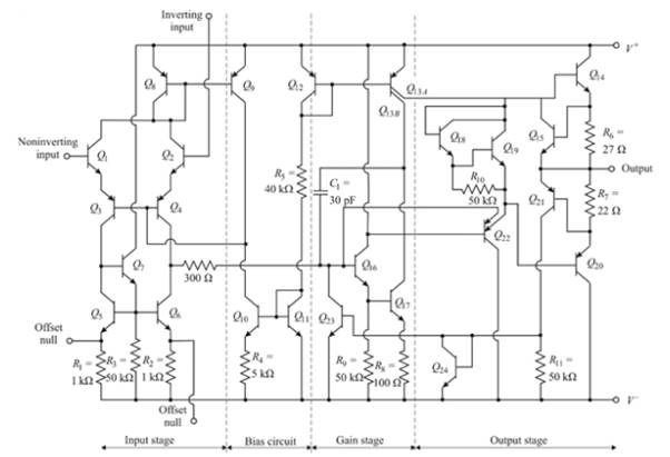
  Microelectronics: Circuit Analysis and Design, Chapter 13, Problem 13.21P

Calculation:

The early voltage given as VA=100V

The reference current is

  IREF=V+VEB12VBE11VR5=50.60.6(5)40=101.240

  =8.840=0.22mA

Current IC10 is.

  IC10R4=VTln(IRFFIC10)IC10(5×10³)=(0.026)ln(0.22×10³IC10)IC10=(0.026)5×10³ln(0.22×10³IC10)=(5.2×10³)ln(0.22×10³IC10)By trial and error method,IC10=14.20μA

The bias currents in the input stage are,

  IC1=IC2=IC3=IC4=IC102=14.20×1062=7.10μA

The voltage at the collector of Q6 is,

  VC6=VBE+VBE6+IC6R2+V=0.6+0.6+(0.0071×10³)(1×10³)+(5)=1.2+0.00715=3.79VC63.8V

The collector current in Q17 is

  IC17=IC13B=0.75IREF=0.75×0.22×103=0.165mA .

Now, current IC13A is,

  IC13A=(0.25)IREF=(0.25)(0.22×10³)=0.055mA

Assuming βn=200 for the npn device, the base current in Q17 is

  IB17=IC17βn=0.165200=0.000825mA

The current in Q16 is

  IC16=IB17+IE17R8+VBF17R9

  =0.000825×10³+(0.165×10³)(0.1×10³)+0.650×103=0.000825×10³+0.616550×103=0.000825×10³+0.01233×10³IC16=0.0132mA

The input resistance to the gain stage is found as

  rπ17=βnVTIC17=200×0.0260.165×103=31.51

Therefore, the emitter resistor RE is

  RE=R9[rπ17+(1+βn)R8]=50×103[31.5×10³+(1+200)(0.1×10³)]=50×103[31.5×10³+(201)(0.1×10³)]

  =50×103[31.5×10³+20.1×10³]=50×103[51.6×10³]=(50×103)(51.6×10³)50×103+51.6×103=25.39×10³RE=25.4

Also,

  rπ16=βnVTIC16=(200)(0.026)0.0132×103=394

Consequently, the resistor value Ri2 is

  Ri2=rπ16+(1+βn)RE=394×103+(1+200)25.4×103=394×103+(201)25.4×103=394×103+5105.4×103=5499.4×103Ri2=5.50

Now the resistance of the active load is determined as

  rπ6=βnVTIC6=200×0.0260.0071×103=732gπ6=IC6Vr=0.0071×1030.026=0.273mA/V

And

  ro6=VAIC6=1000.0071×103=14.08

Then,

  Roct=ro6[1+gm6(R2rπ6)]=(14.08×10⁶)[1+0.273×10³(1×103732×103)]

  =(14.08×10⁶)[1+(0.273×10³)(1×103×732×1031×103+732×103)]

  =(14.08×10⁶)[1+(0.273×10³)(732733×103)]=(14.08×10⁶)[1+(0.273)(0.998)]

  =(14.08×10⁶)(1+0.2726)=(14.08×10⁶)(1.2726)

  Roct=17.93

Now the resistance ro4 is

  ro4=VAIC4=1000.0071×103=14.08

The small signal differential voltage is

  Ad=gm1(ro4Roct1Ri2)=(7.10×1060.026)(14.08×10617.93×1065.5×106)

  =(273.07×10³)((14.08×10⁶)(17.93×10⁶)14.08×10⁶+17.93×1065.5×106)

  =(273.07×10³)(252.4544×10632.015.5×106)=(273.07×10³)(7.886×1065.5×106)

  =(273.07×10³)((7.886×10⁶)(5.5×10⁶)7.886×10⁶+5.5×10⁶)=(273.07×10³)(43.37313.386×106)=(273.07×10³)(3.240×10⁶)=885

The effective resistance of the active load is the resistance looking into the collector of Q13B is

  Roct2=ro13B=VAIC13B=1000.165×103=606

And the output resistance Ro17 is

  Ro17=VAIC17=1000.165×103=606

The small signal voltage gain is

  Av2=βn(1+βn)R9(Roct2Ro17)Ri2{R9+[rπ17+(1+βn)R8]}

  =200(1+200)50×103(606×103606×103)5500×103{50×103+[31.5×10³+(1+200)(0.1×10³)]}

  =200(201)(50×103)(606×606×103606+606)5500×103{50×103+[31.5×10³+(201)(0.1×10³)]}

  =40200×50×103(3672361212×103)5500×103{50×103+[31.5×10³+20.1×10³]}

  =(40200)(50×103)(3672361212×103)5500×103{50×103+51.6×10³}

  =(40200)(50×103)(303×103)5500×103{101.6×10³}=40200×15150556050

  =1090

  Av2=1090

The overall gain is

  Av=Ad×An=(885)(1090)=964650

  Av=964650

Want to see more full solutions like this?

Subscribe now to access step-by-step solutions to millions of textbook problems written by subject matter experts!

Chapter 13 Solutions

Microelectronics: Circuit Analysis and Design

Ch. 13 - Prob. 13.11EPCh. 13 - Prob. 13.10TYUCh. 13 - Prob. 13.12TYUCh. 13 - Prob. 13.12EPCh. 13 - Prob. 13.13EPCh. 13 - Prob. 13.15EPCh. 13 - Prob. 13.15TYUCh. 13 - Consider the LF155 BiFET input stage in Figure...Ch. 13 - Describe the principal stages of a generalpurpose...Ch. 13 - Prob. 2RQCh. 13 - Prob. 3RQCh. 13 - Describe the operation and characteristics of a...Ch. 13 - Describe the configuration and operation of the...Ch. 13 - What is the purpose of the resistorin the active...Ch. 13 - Prob. 7RQCh. 13 - Prob. 8RQCh. 13 - Describe the frequency compensation technique in...Ch. 13 - Sketch and describe the general characteristics of...Ch. 13 - Prob. 11RQCh. 13 - Sketch and describe the principal advantage of a...Ch. 13 - Prob. 13RQCh. 13 - What are the principal factors limiting the...Ch. 13 - Consider the simple MOS opamp circuit shown in...Ch. 13 - Prob. 13.2PCh. 13 - Prob. 13.5PCh. 13 - Consider the input stage of the 741 opamp in...Ch. 13 - Prob. 13.7PCh. 13 - Prob. 13.8PCh. 13 - Prob. 13.10PCh. 13 - The minimum recommended supply voltages for the...Ch. 13 - Prob. 13.12PCh. 13 - Consider the 741 opamp in Figure 13.3, biased with...Ch. 13 - Prob. 13.14PCh. 13 - Consider the output stage of the 741 opamp shown...Ch. 13 - Prob. 13.16PCh. 13 - Prob. 13.19PCh. 13 - Prob. 13.20PCh. 13 - Prob. 13.21PCh. 13 - Prob. 13.22PCh. 13 - Prob. 13.23PCh. 13 - Prob. 13.24PCh. 13 - (a) Determine the differential input resistance of...Ch. 13 - An opamp that is internally compensated by Miller...Ch. 13 - The CMOS opamp in Figure 13.14 is biased at V+=5V...Ch. 13 - Prob. 13.34PCh. 13 - Consider the MC14573 opamp in Figure 13.14, with...Ch. 13 - Prob. 13.36PCh. 13 - Prob. 13.37PCh. 13 - Prob. 13.39PCh. 13 - Prob. 13.41PCh. 13 - In the bias portion of the CA1340 opamp in Figure...Ch. 13 - Prob. 13.57PCh. 13 - In the LF155 BiFET opamp in Figure 13.25, the...
Knowledge Booster
Background pattern image
Electrical Engineering
Learn more about
Need a deep-dive on the concept behind this application? Look no further. Learn more about this topic, electrical-engineering and related others by exploring similar questions and additional content below.
Recommended textbooks for you
Text book image
Introductory Circuit Analysis (13th Edition)
Electrical Engineering
ISBN:9780133923605
Author:Robert L. Boylestad
Publisher:PEARSON
Text book image
Delmar's Standard Textbook Of Electricity
Electrical Engineering
ISBN:9781337900348
Author:Stephen L. Herman
Publisher:Cengage Learning
Text book image
Programmable Logic Controllers
Electrical Engineering
ISBN:9780073373843
Author:Frank D. Petruzella
Publisher:McGraw-Hill Education
Text book image
Fundamentals of Electric Circuits
Electrical Engineering
ISBN:9780078028229
Author:Charles K Alexander, Matthew Sadiku
Publisher:McGraw-Hill Education
Text book image
Electric Circuits. (11th Edition)
Electrical Engineering
ISBN:9780134746968
Author:James W. Nilsson, Susan Riedel
Publisher:PEARSON
Text book image
Engineering Electromagnetics
Electrical Engineering
ISBN:9780078028151
Author:Hayt, William H. (william Hart), Jr, BUCK, John A.
Publisher:Mcgraw-hill Education,
Differential Amplifiers Made Easy; Author: The AudioPhool;https://www.youtube.com/watch?v=Mcxpn2HMgtU;License: Standard Youtube License