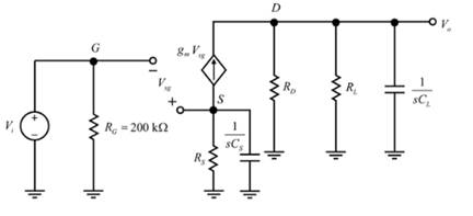
In the common−source amplifier in Figure 7.25(a) in the text, a source bypass capacitor is to be added between the source terminal and ground potential. The circuit parameters are R S = 3 .2kΩ , R D = 10kΩ , R L = 20kΩ , and C L = 10 pF . The transistor parameters are V T P = − 2 V K P =0 .25mA/V 2 , and λ = 0 . (a) Derive the small−signal voltage gain expression, as a function of s, that describes the circuit behavior in the high−frequency range. (b) What is the expression for the time constant associated with the upper 3dB frequency? (c) Determine the time constant, upper 3dB frequency, and small−signal midband voltage gain.
In the common−source amplifier in Figure 7.25(a) in the text, a source bypass capacitor is to be added between the source terminal and ground potential. The circuit parameters are R S = 3 .2kΩ , R D = 10kΩ , R L = 20kΩ , and C L = 10 pF . The transistor parameters are V T P = − 2 V K P =0 .25mA/V 2 , and λ = 0 . (a) Derive the small−signal voltage gain expression, as a function of s, that describes the circuit behavior in the high−frequency range. (b) What is the expression for the time constant associated with the upper 3dB frequency? (c) Determine the time constant, upper 3dB frequency, and small−signal midband voltage gain.
In the common−source amplifier in Figure 7.25(a) in the text, a source bypass capacitor is to be added between the source terminal and ground potential. The circuit parameters are
R
S
=
3
.2kΩ
,
R
D
=
10kΩ
,
R
L
=
20kΩ
, and
C
L
=
10
pF
. The transistor parameters are
V
T
P
=
−
2
V
K
P
=0
.25mA/V
2
, and
λ
=
0
. (a) Derive the small−signal voltage gain expression, as a function of s, that describes the circuit behavior in the high−frequency range. (b) What is the expression for the time constant associated with the upper 3dB frequency? (c) Determine the time constant, upper 3dB frequency, and small−signal midband voltage gain.
a.
Expert Solution
To determine
To derive: The small signal voltage gain expression.
Answer to Problem 7.41P
The expression for small signal voltage gain:
Av=−gm(RD𑨈RL)[1+gm(Rs𑨈(1sCs))](11+s(RD𑨈RL)CL)
Explanation of Solution
Given:
The circuit parameter is given as:
RS=3.2kΩRD=10kΩRL=20kΩCL=10pF
The transistor parameter are given as:
VTP=−2VKP=0.25mA/V2λ=0
Drawing the small signal model of the circuit with the source bypass capacitor:
Applying the Ohm’s law to the drain terminal:
V0=gmVsg(RD𑨈RL𑨈1sCL)
Evaluating the input voltage Vi :
Vi=−Vsg−gmVsg(Rs𑨈(1sCs))=−Vsg[1+gm(Rs𑨈(1sCs))]
Evaluating the ratio of output voltage to the input voltage:
A circuit consist of two cascaded opamp amplifiers, If the gain of first stage is 6.7 and the gain of the second
stage is 3.
Then the total voltage gain A, is
Moving to another question will save this response.
Quèstion 7
In ac analysis of transistor biasing circuits, coupling capacitors should be open circuit.
True
False
Moving to another question will save this response.
nere to search
O
a
5. MOSFET circuit
The MOSFET in the circuit below has V = 0.5 V and kn
= 0.4 mA/V². Determine Vout-
+ 5 V
1 mA
o Vout
Need a deep-dive on the concept behind this application? Look no further. Learn more about this topic, electrical-engineering and related others by exploring similar questions and additional content below.


 Introductory Circuit Analysis (13th Edition)Electrical EngineeringISBN:9780133923605Author:Robert L. BoylestadPublisher:PEARSON
 Delmar's Standard Textbook Of ElectricityElectrical EngineeringISBN:9781337900348Author:Stephen L. HermanPublisher:Cengage Learning
 Programmable Logic ControllersElectrical EngineeringISBN:9780073373843Author:Frank D. PetruzellaPublisher:McGraw-Hill Education
 Fundamentals of Electric CircuitsElectrical EngineeringISBN:9780078028229Author:Charles K Alexander, Matthew SadikuPublisher:McGraw-Hill Education
 Electric Circuits. (11th Edition)Electrical EngineeringISBN:9780134746968Author:James W. Nilsson, Susan RiedelPublisher:PEARSON
 Engineering ElectromagneticsElectrical EngineeringISBN:9780078028151Author:Hayt, William H. (william Hart), Jr, BUCK, John A.Publisher:Mcgraw-hill Education,