Loose Leaf for Engineering Circuit Analysis Format: Loose-leaf
9th Edition
ISBN: 9781259989452
Author: Hayt
Publisher: Mcgraw Hill Publishers
expand_more
expand_more
format_list_bulleted
Concept explainers
Videos
Textbook Question
Chapter 3, Problem 12E
For the circuit of Fig. 3.55 (which employs a model for the dc operation of a bipolar junction transistor biased in active region), IC is measured to be 1.5 mA. Calculate IB and IE.
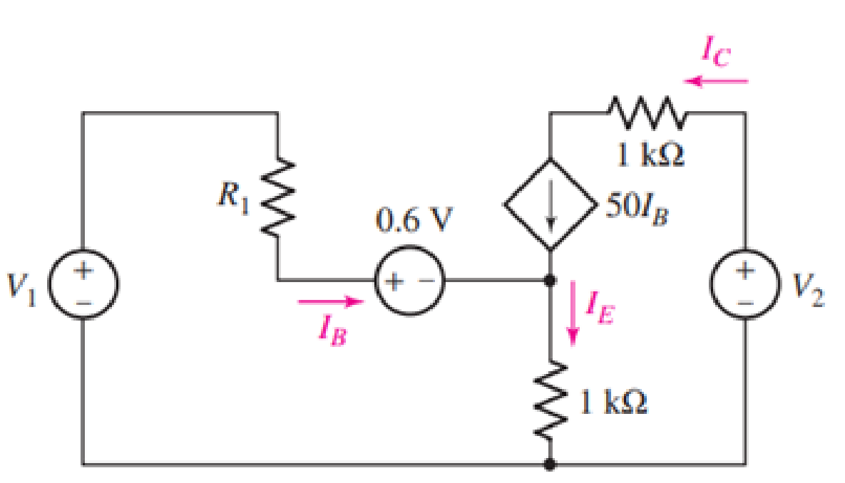
FIGURE 3.55
Expert Solution & Answer
Want to see the full answer?
Check out a sample textbook solution
Students have asked these similar questions
Example 3.1
nje (in claku sheet.
1/
The transistor in the circuit (a) has ß=100 and VBE=0.7V @ ic-1mA. Design the
circuit so that a current of 2mA flows through the collector and a voltage of +5V
appears at the collector, i.e. determine the values of RC and RE for the circuit
(5k2 and 7k).
+15 V
2MA
OV
(a)
10V
+5V
Rc
-0.70
-15 V
RE
210TEWODU2MDM0/a/Mjg2ODQOMZMyOTc3/details
202
Open with Google Docs
3. The network of Figure below is the basic biasing arrangement for the field-effect transistor (FET), a
device of increasing importance in electronic design. (Biasing simply means the application of de
levels to establish a particular set of operating conditions.) Even though you may be unfamiliar with
the FET, you can perform the following analysis using only the basic laws introduced in your lectures
and the information provided on the diagram.
a. Determine the voltages VG and Vs.
b. Find the currents I, 12, Ip, and Is.
c. Determine Ds.
d. Calculate V DG:
VDD = 16 V
오
ID
R1
2 MO
RD
C2.5 kfl
OD
G
I IG
I'Gs =-1.75 V
I6 = 0 A
Ip Is
R
270 kf?
Is
Rs 15 k2
ctivate
Page 1 2
o to Setti
: For the given circuit, transistors and diodes are silicon where VD₁=VD2=0.7V
and |VBE|=0.7V. Neglect base currents.
a) Calculate VB1, VB2 which are base to ground DC voltages of Q1 and Q2, respectively
b) Calculate the power generated by source
c) Calculate the maximum power delivered to load and conversion efficiency
Show your calculations step by step and fill the table. (Or you can draw the same
table in your answer sheet).
No
▷
D₁
D₂
1K
Q₁
+20V
C
HH
RL=1002
a) VB₁[V]
VB2 [V]
b) PDC [W]
c) PL[W]
Efficiency
Chapter 3 Solutions
Loose Leaf for Engineering Circuit Analysis Format: Loose-leaf
Ch. 3.2 - 3.1 (a) Count the number of branches and nodes in...Ch. 3.3 - Determine ix and vx in the circuit of Fig. 3.7....Ch. 3.3 - For the circuit of Fig. 3.9, if vR1=1V, determine...Ch. 3.3 - Determine vx in the circuit of Fig. 3.11.Ch. 3.4 - In the circuit of Fig. 3.12b, vs1 = 120 V, vs2 =...Ch. 3.4 - 3.6 In the circuit of Fig. 3.14, find the power...Ch. 3.5 - Determine v in the circuit of Fig. 3.16.Ch. 3.5 - For the single-node-pair circuit of Fig. 3.18,...Ch. 3.6 - Determine the current i in the circuit of Fig....Ch. 3.6 - Determine the voltage v in the circuit of Fig....
Ch. 3.6 - Determine whether the circuit of Fig. 3.25...Ch. 3.7 - 3.12 Determine a single-value equivalent...Ch. 3.7 - 3.13 Determine i in the circuit of Fig. 3.29....Ch. 3.7 - Determine v in the circuit of Fig. 3.31 by first...Ch. 3.7 - 3.15 For the circuit of Fig. 3.33, calculate the...Ch. 3.8 - 3.16 Use voltage division to determine vx in the...Ch. 3.8 - In the circuit of Fig. 3.40, use resistance...Ch. 3 - Referring to the circuit depicted in Fig. 3.45,...Ch. 3 - Referring to the circuit depicted in Fig. 3.46,...Ch. 3 - For the circuit of Fig. 3.47: (a) Count the number...Ch. 3 - For the circuit of Fig. 3.47: (a) Count the number...Ch. 3 - Refer to the circuit of Fig. 3.48, and answer the...Ch. 3 - A local restaurant has a neon sign constructed...Ch. 3 - Referring to the single-node diagram of Fig. 3.50,...Ch. 3 - Determine the current labeled I in each of the...Ch. 3 - In the circuit shown in Fig. 3.52, the resistor...Ch. 3 - The circuit of Fig. 3.53 represents a system...Ch. 3 - In the circuit depicted in Fig. 3.54, ix is...Ch. 3 - For the circuit of Fig. 3.55 (which employs a...Ch. 3 - Determine the current labeled I3 in the circuit of...Ch. 3 - Study the circuit depicted in Fig. 3.57, and...Ch. 3 - Prob. 15ECh. 3 - For the circuit of Fig. 3.58: (a) Determine the...Ch. 3 - For each of the circuits in Fig. 3.59, determine...Ch. 3 - Use KVL to obtain a numerical value for the...Ch. 3 - Prob. 19ECh. 3 - In the circuit of Fig. 3.55, calculate the voltage...Ch. 3 - Determine the value of vx as labeled in the...Ch. 3 - Consider the simple circuit shown in Fig. 3.63....Ch. 3 - (a) Determine a numerical value for each current...Ch. 3 - The circuit shown in Fig. 3.65 includes a device...Ch. 3 - The circuit of Fig. 3.12b is constructed with the...Ch. 3 - Obtain a numerical value for the power absorbed by...Ch. 3 - Compute the power absorbed by each element of the...Ch. 3 - Compute the power absorbed by each element in the...Ch. 3 - Kirchhoffs laws apply whether or not Ohms law...Ch. 3 - Referring to the circuit of Fig. 3.70, (a)...Ch. 3 - Determine a value for the voltage v as labeled in...Ch. 3 - Referring to the circuit depicted in Fig. 3.72,...Ch. 3 - Determine the voltage v as labeled in Fig. 3.73,...Ch. 3 - Although drawn so that it may not appear obvious...Ch. 3 - Determine the numerical value for veq in Fig....Ch. 3 - Determine the numerical value for ieq in Fig....Ch. 3 - For the circuit presented in Fig. 3.76. determine...Ch. 3 - Determine the value of v1 required to obtain a...Ch. 3 - (a) For the circuit of Fig. 3.78, determine the...Ch. 3 - What value of IS in the circuit of Fig. 3.79 will...Ch. 3 - (a) Determine the values for IX and VY in the...Ch. 3 - Determine the equivalent resistance of each of the...Ch. 3 - For each network depicted in Fig. 3.82, determine...Ch. 3 - (a) Simplify the circuit of Fig. 3.83 as much as...Ch. 3 - (a) Simplify the circuit of Fig. 3.84, using...Ch. 3 - Making appropriate use of resistor combination...Ch. 3 - Calculate the voltage labeled vx in the circuit of...Ch. 3 - Determine the power absorbed by the 15 resistor...Ch. 3 - Calculate the equivalent resistance Req of the...Ch. 3 - Show how to combine four 100 resistors to obtain...Ch. 3 - Prob. 51ECh. 3 - Prob. 52ECh. 3 - Prob. 53ECh. 3 - Prob. 54ECh. 3 - Prob. 55ECh. 3 - Prob. 56ECh. 3 - Prob. 57ECh. 3 - Prob. 58ECh. 3 - Prob. 59ECh. 3 - Prob. 60ECh. 3 - With regard to the circuit shown in Fig. 3.98,...Ch. 3 - Delete the leftmost 10 resistor in the circuit of...Ch. 3 - Consider the seven-element circuit depicted in...
Knowledge Booster


Learn more about
Need a deep-dive on the concept behind this application? Look no further. Learn more about this topic, electrical-engineering and related others by exploring similar questions and additional content below.Similar questions
- 3. Given the circuit in figure 3.1 below. 3.1 Calculate the value of RC to obtain a collector current IC = 4mA 3.2 Find the corresponding value of VCE with the proposed RC value in part 3.1. Vcc = 20V Rc lc R1 4KQ VBE= 0.5 V Q:VCE Beta= 80 R2 5KO RE 2002 Figure 3.1 The bipolar junction transistor the circuitarrow_forwardThe silicon transistor shown in the figure below has reverse saturation current of 10-9 A. If VBE = 0.7 V, then the value of current 'T will be mA. (Assume V7= 26 mV, n = 2)arrow_forward3.20. In the following circuit, find the minimum Vịn required and the resulting voltage Vout to put the transistor in full saturation. Assume that the ß for the transistor is 100 in full saturation. Vs = 5 V Rc = 1kQ Rg = 1k2 Vout Vin Rout = 1k2arrow_forward
- 2. Explain the operation and Analyse the performance of a range of discrete semiconductor devices used in modern electronic systems in terms of simple semiconductor theory, and suggesting appropriate applications for each, such as: Transistor ● Triac ● MOSFET Thyristorsarrow_forwardFor the circuit shown find: a. Power consumed in RL b. DC voltage of current source Ip dc. c. Q points of operation of the 2 transistors If it is not possible to calculate explain by laws. ID = 3 milliamperes. All semiconductors are silicon. Vcc 12 V BETA=100 ID Q1 D1 D2 Q2 100 Q D, 10 k2 VEE - 12 Varrow_forwardIN OUT GND V3 (1) R VR Consider the design of a DC power supply as shown above with the following requirements and constraints: • input from a 240 V RMS 50 Hz mains supply • diodes have a forward voltage drop of 0.6 V • utput voltage is required to be 9.1 V supplying a current of 575 mA • uses a 20:1 step-down transformer • the voltage regulator has a dropout voltage of 1.8 V In all of the questions below, give numeric answers correct to 3 significant figures and include units where required. Keep track of your intermediate results to more significant figures, otherwise rounding errors may lead to incorrect results. a. What is the peak voltage available at the secondary windings of the transformer? 数字 单位 b. What is the peak voltage across the filter capacitor? 数字 单位 c. What is the minimum allowable voltage at the input of the voltage regulator? 数字 单位 d. What is the maximum allowable allowable ripple voltage across the capacitor? 数字 单位 e. What is the minimum capacitor value that will…arrow_forward
- below diagramshows a silicon transistor with B = 100 biased by base resistor method. Draw the d.cloadline and determine the operating point. %3Darrow_forwardCalculate the resistance value, Rs needed for a p-channel JFET transistor circuit if you know that IDss = 25 mA, VGSS (off) = 15V, and VGs = 5V. %3Darrow_forwardQ3.12: Consider the circuit of Fig (3.12), and assume that the two diodes are identical and that they each have Zener Voltage of 5.8 V. (a) Determine the output limiting voltage. (b) Determine the input limiting Voltage. (c) For Vin = 0.5 V, determine Vo, i, iRizgandio (d) For Vin = 15V; repeat calculations of (C). Ans /(a) Vo iR eis Vin = 2 TOK -www iR=i = 50 MA N LR 好 100 K Lo 2 = 58 MA 9 iz = 1.442 mA, Vo 7 5.8 V₂ (b) Vin = I 0.58 V, (C) V₁ = -5V₂ x ₁ = 50 MA Az=o (d) Vo= -5.8V, ₁ = 1.5 mA, do = i. = 1.5 mA - Fig (3.12)arrow_forward
- Q2 Design a voltage divider bias circuit for an npn silicon transistor having B %D 100 to be used in a Common Emitter configuration. The quiescent point = 1 mA, VCE = 5 V. The supply voltage (Vcc) is 15 V. (Q point) is to be l. Assume VĘ = 0.1Vcc and BRĘ 2 10R2. (a)Find all the resistors values and draw the schematic diagram of this Common Emitter Amplifier with bypass capacitor CE.arrow_forward21. The below picture shows a complete npn transistor. In creating this transistor, silicon doped with phosphorus is made into a polished wafer first. What is the next step in the manufacturing process? ➤ a. Doping with a p type chemical b. Etching c. Growing the SiO2 layer d. Apply photoresist n nt Р n Al SiO₂ narrow_forwardQuestion 3.31 Determine the region of operation for a transistor whose characteristics are those of Fig. 3.8 if ICmax 6 mA, VCBmax=15 V and PCmax= 30 mW.arrow_forward
arrow_back_ios
SEE MORE QUESTIONS
arrow_forward_ios
Recommended textbooks for you
 Introductory Circuit Analysis (13th Edition)Electrical EngineeringISBN:9780133923605Author:Robert L. BoylestadPublisher:PEARSON
 Delmar's Standard Textbook Of ElectricityElectrical EngineeringISBN:9781337900348Author:Stephen L. HermanPublisher:Cengage Learning
 Programmable Logic ControllersElectrical EngineeringISBN:9780073373843Author:Frank D. PetruzellaPublisher:McGraw-Hill Education
 Fundamentals of Electric CircuitsElectrical EngineeringISBN:9780078028229Author:Charles K Alexander, Matthew SadikuPublisher:McGraw-Hill Education
 Electric Circuits. (11th Edition)Electrical EngineeringISBN:9780134746968Author:James W. Nilsson, Susan RiedelPublisher:PEARSON
 Engineering ElectromagneticsElectrical EngineeringISBN:9780078028151Author:Hayt, William H. (william Hart), Jr, BUCK, John A.Publisher:Mcgraw-hill Education,
Introductory Circuit Analysis (13th Edition)
Electrical Engineering
ISBN:9780133923605
Author:Robert L. Boylestad
Publisher:PEARSON
Delmar's Standard Textbook Of Electricity
Electrical Engineering
ISBN:9781337900348
Author:Stephen L. Herman
Publisher:Cengage Learning
Programmable Logic Controllers
Electrical Engineering
ISBN:9780073373843
Author:Frank D. Petruzella
Publisher:McGraw-Hill Education
Fundamentals of Electric Circuits
Electrical Engineering
ISBN:9780078028229
Author:Charles K Alexander, Matthew Sadiku
Publisher:McGraw-Hill Education
Electric Circuits. (11th Edition)
Electrical Engineering
ISBN:9780134746968
Author:James W. Nilsson, Susan Riedel
Publisher:PEARSON
Engineering Electromagnetics
Electrical Engineering
ISBN:9780078028151
Author:Hayt, William H. (william Hart), Jr, BUCK, John A.
Publisher:Mcgraw-hill Education,
Current Divider Rule; Author: Neso Academy;https://www.youtube.com/watch?v=hRU1mKWUehY;License: Standard YouTube License, CC-BY